Solar Panel Manufacturing: A Deep Dive Into Materials, Process & Machinery
Solar panel manufacturing is the industrial process used to transform semiconductor materials and other components into photovoltaic (PV) modules that convert sunlight into electricity. The process involves several connected stages, beginning with raw silicon and continuing through wafer production, solar cell fabrication, module assembly, testing, and quality control.
Context
Crystalline silicon remains a major technology in photovoltaic manufacturing. A typical silicon-based supply chain includes polysilicon, silicon ingots, wafers, solar cells, and finished modules. Other photovoltaic technologies use materials such as cadmium telluride, copper indium gallium diselenide, or emerging perovskite materials. NREL describes crystalline-silicon production as involving polysilicon processing, ingot and wafer production, cell conversion, and module assembly, while thin-film and tandem technologies follow different manufacturing routes.
A finished solar module contains more than solar cells. Depending on its design, it can include glass, encapsulation materials, electrical conductors, a backsheet or second glass layer, an aluminum frame, and a junction box. These components work together to protect the cells and provide electrical connections.
Main stages of solar panel manufacturing
The overall manufacturing chain can be viewed as a sequence:
- Polysilicon preparation
- Ingot formation
- Wafer slicing and preparation
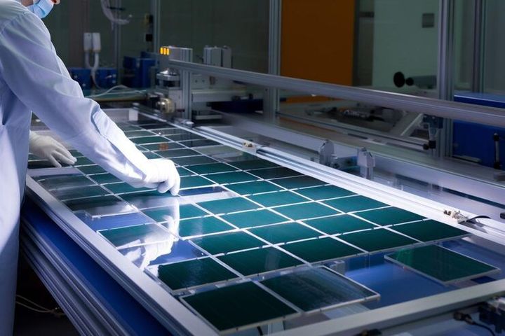
- Solar cell fabrication
- Cell testing and sorting
- Cell interconnection
- Module lamination
- Framing and junction-box installation
- Electrical and environmental testing
The exact sequence and machinery vary according to the cell architecture and module design.
Materials used in solar panels
Silicon is the central semiconductor material for most crystalline-silicon panels. High-purity silicon is formed into ingots and sliced into thin wafers before the wafers are processed into photovoltaic cells.
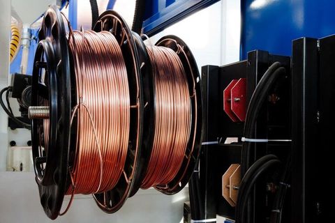
Other important materials include glass, aluminum, copper, silver-based or other conductive metallization materials, encapsulants, backsheets, junction-box components, and adhesives. Material selection influences electrical performance, mechanical strength, environmental resistance, manufacturing yield, and recyclability.
Importance
Solar panel manufacturing matters because photovoltaic modules are manufactured through a complex chain that connects semiconductor processing, precision machinery, electrical engineering, materials science, and quality control.
As photovoltaic deployment expands, manufacturing capacity has also grown. The IEA PVPS reported that global cumulative PV capacity reached nearly 3 TW by the end of 2025, with about 690 GW of new capacity installed during that year. The same report noted continued manufacturing overcapacity, meaning available production capability exceeded annual module installations.
For everyday users, manufacturing quality matters because a photovoltaic module operates outdoors for many years under changing temperatures, moisture, mechanical loads, and sunlight. Manufacturing defects can therefore affect electrical performance and long-term reliability.
Why production quality matters
Several manufacturing variables require close control:
- Wafer thickness and surface condition
- Cell electrical characteristics
- Metallization quality
- Soldering or interconnection quality
- Encapsulant bonding
- Lamination conditions
- Glass and frame alignment
- Junction-box attachment
- Electrical insulation
- Final module testing
Quality control is performed at multiple stages rather than only after a module has been assembled. This approach allows manufacturers to identify process variations before they affect later production stages.
Solar panel manufacturing technologies
Different cell architectures require different processing steps and machinery. PERC, TOPCon, heterojunction technology (HJT), interdigitated back-contact (IBC), and other designs use variations in wafer treatment, surface passivation, doping, metallization, and interconnection.
NREL identifies several crystalline-silicon cell approaches, including PERC, TOPCon, HJT, and IBC, along with different approaches to module assembly such as conventional stringing, busbarless designs, and shingling.
| Manufacturing stage | Main material or input | Typical equipment function |
|---|---|---|
| Polysilicon processing | High-purity silicon | Chemical purification and deposition |
| Ingot production | Polysilicon | Crystal growth and solidification |
| Wafer production | Silicon ingot | Cutting, shaping and surface preparation |
| Cell processing | Silicon wafer | Texturing, doping, passivation and metallization |
| Cell interconnection | Finished cells | Stringing or other electrical connection |
| Module assembly | Cells, glass, encapsulants | Lay-up, lamination and assembly |
| Final testing | Completed module | Electrical, visual and safety evaluation |
Recent Updates
Solar panel manufacturing has been changing rapidly through improvements in silicon cell architecture, wafer formats, module design, automation, and emerging photovoltaic technologies.
Recent IEA PVPS data indicates that n-type technologies have continued to gain market share. In 2025, n-type wafers represented around 82% of crystalline-silicon wafers used for cell manufacturing. The same report also identified continued manufacturing overcapacity across the global module industry.
TOPCon and HJT development
TOPCon and HJT have received substantial industrial attention as manufacturers transition from older cell architectures toward newer designs. Manufacturing improvements include changes in passivation, metallization, wafer handling, and production-line automation.
The shift toward n-type wafers also affects machinery because different cell architectures require specific deposition, cleaning, laser-processing, metallization, and inspection equipment.
Perovskite and tandem research
Perovskite photovoltaic technology has received significant research attention because it can be combined with crystalline silicon to create tandem cells. A tandem structure places photovoltaic materials with different light-absorption characteristics together so that more portions of the solar spectrum can be converted.
IEA PVPS reported that pilot production and demonstration activity for perovskite technologies continued during the recent period, while large-scale commercial production had not yet been established across the sector. Research into perovskite-silicon tandem structures has also continued.
This distinction is important: laboratory records, pilot production, and established high-volume manufacturing are different stages of technological development.
Automation and digital manufacturing
Automation is increasingly used for wafer handling, cell inspection, module assembly, equipment control, and production data collection. Machine-vision systems can identify visible defects, while automated electrical testing can measure characteristics of individual cells and completed modules.
Digitalization is also expanding beyond factory equipment. IEA PVPS reported growing interest in digital twins, artificial intelligence, Internet of Things technologies, standardized data structures, and cybersecurity across the photovoltaic value chain.
Greater attention to environmental data
Environmental assessment has also become more data-driven. In 2026, IEA PVPS published an updated photovoltaic life-cycle inventory covering newer datasets for technologies including TOPCon and PERC crystalline-silicon supply chains and CdTe modules. Such inventories help researchers assess material flows, energy use, and emissions associated with different photovoltaic technologies.
Laws or Policies
Solar panel manufacturing is influenced by several types of regulations and technical requirements. Because requirements differ between jurisdictions, a manufacturer cannot assume that one regulatory framework applies everywhere.
Common regulatory areas include:
- Electrical and product safety
- Factory and worker protection
- Environmental emissions and waste management
- Chemical handling
- Import and export requirements
- Product labeling and documentation
- Recycling or end-of-life requirements
- Quality and conformity assessment
International standards are also widely used as technical references. IEC 61215 establishes design-qualification and type-approval testing for terrestrial photovoltaic modules, while IEC 61730 addresses fundamental construction and safety requirements. The current IEC 61730-1:2023 publication states that its requirements do not encompass every national or regional code, which means local requirements still need to be considered.
IEC 62941 addresses quality systems for photovoltaic module manufacturing. It covers product and process design as well as control of materials and manufacturing processes for relevant certified modules.
These standards should not be treated as a universal legal checklist. Actual obligations depend on the location of the manufacturing facility, the destination market, the product type, and applicable regulatory authorities.
Tools and Resources
Several technical resources can help readers understand solar panel manufacturing without requiring specialist manufacturing knowledge.
PV manufacturing research
The National Renewable Energy Laboratory publishes technical material covering silicon photovoltaics, cell technologies, manufacturing processes, materials, and module designs. Its resources can help explain how individual production stages connect with one another.
IEA PVPS reports
IEA PVPS publishes research covering photovoltaic deployment, manufacturing, technology development, life-cycle assessment, recycling, degradation, and digitalization. Its recent reports provide information about global industry trends and emerging technologies.
IEC standards
IEC publications can be used to understand internationally recognized approaches to photovoltaic module qualification, safety, and manufacturing quality. Manufacturers and technical teams generally need to identify the specific editions and requirements relevant to their product and market.
Manufacturing monitoring tools
Factories may use several categories of monitoring equipment, including:
- Wafer inspection systems
- Cell electroluminescence imaging
- Surface inspection cameras
- Solar simulators
- Electrical performance testers
- Lamination monitoring systems
- Environmental and process sensors
- Production-data management systems
These tools help manufacturers identify defects and monitor consistency across production stages.
FAQs
What is involved in solar panel manufacturing?
Solar panel manufacturing can involve polysilicon preparation, ingot growth, wafer production, cell processing, electrical interconnection, module assembly, lamination, framing, junction-box installation, and final testing. The exact process depends on the photovoltaic technology being produced.
What materials are used in solar panel manufacturing?
Crystalline-silicon panels commonly use silicon wafers together with glass, encapsulation materials, aluminum, copper, conductive metallization materials, backsheets or rear glass, and junction-box components. Thin-film technologies use different semiconductor materials.
What machinery is used in solar panel manufacturing?
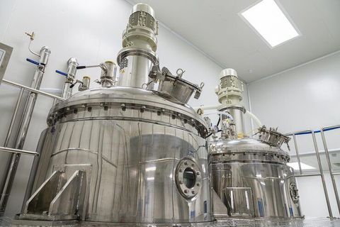
Machinery varies by production stage. Equipment can include crystal-growth furnaces, wafer saws, cleaning and texturing systems, diffusion or deposition equipment, laser-processing systems, screen printers, cell testers, stringers, laminators, framing equipment, junction-box assembly equipment, and module inspection systems.
What is the difference between TOPCon, HJT and PERC solar cells?
TOPCon, HJT, and PERC are different crystalline-silicon cell architectures. They use different combinations of surface passivation, semiconductor layers, wafer treatment, and electrical contacts. These differences affect the required manufacturing steps and production equipment.
Are perovskite solar panels commercially manufactured?
Perovskite photovoltaic technology has progressed through research, pilot production, and demonstration activities. However, IEA PVPS reported that large-scale commercial production had not yet been established for the emerging perovskite technologies discussed in its recent review.
Conclusion
Solar panel manufacturing combines semiconductor processing, materials engineering, precision machinery, automation, module assembly, and quality testing. Crystalline silicon remains a major photovoltaic technology, while TOPCon, HJT, back-contact designs, perovskite cells, and tandem structures continue to shape research and manufacturing development. Recent industry trends also show greater attention to automation, digital monitoring, life-cycle data, and supply-chain structure. Manufacturing requirements are influenced by technical standards and local regulations, so the applicable requirements depend on the product and jurisdiction.